
DDR5, the fifth-gen DRAM, calls for digital-analogue finesse in its MC and DDR PHY. Distinctive timings, coupled with rising tech like 3D XPoint, MRAM, and ReRAM, mark a paradigm shift
Reminiscence is often used for storing the info or program code wanted by a pc processor to perform. To perform this process, Dynamic random entry reminiscence (DRAM) is employed. DRAM is a typical sort of random entry reminiscence (RAM) utilized in private computer systems (PCs), workstations, and servers. Random entry permits the PC processor to entry any a part of the reminiscence instantly relatively than continuing sequentially from a beginning place.
How does DRAM work?
Reminiscence is fabricated from bits of information or program code organized in a two-dimensional grid. DRAM shops bits of information in what’s referred to as a storage or reminiscence cell, consisting of a capacitor and a transistor. The storage cells are sometimes organised in an oblong configuration. When a cost is distributed by way of a column, the transistor within the column is activated. A DRAM storage cell is dynamic, which means that it must be refreshed or given a brand new digital cost each few milliseconds to compensate for cost leaks from the capacitor.

The reminiscence cells work with different circuits that determine rows and columns, observe the refresh course of, instruct a cell whether or not or to not settle for a cost, and skim or restore information from a cell.
DRAM is one choice of semiconductor reminiscence {that a} system designer can use when constructing a pc. Typical sizes of DRAM are about 1 to 2GB in smartphones and tablets and 4 to 16GB in laptops.
Benefits of DRAM
- Very dense
- Low price per bit
- Easy reminiscence cell construction
Disadvantages of DRAM
- Advanced manufacturing course of
- Knowledge requires refreshing
- Extra advanced exterior circuitry is required (learn and refresh periodically)
- Risky reminiscence
- Comparatively sluggish operational velocity
Manufacturing processes concerned in DRAM
DRAM manufacturing processes are known as 1x-nm, 1y-nm, 1z-nm, 1alpha-nm, and 1-beta. A specific dielectric layer is supplied to attain the capacitance for every bit cell. 1beta DRAMs are low-powered and have double information charge 5X (LPDDR5X), able to delivering information at a charge of 8.5Gbps. Multi-pattern lithography, together with modern course of know-how and superior materials capabilities, is required for the manufacture of 1beta node DRAMs. The introduction of enhanced dynamic voltage and frequency scaling extensions core (eDVFSC) methods is used to enhance power-saving controls of DRAMs.
1-gamma node DRAMs are coming
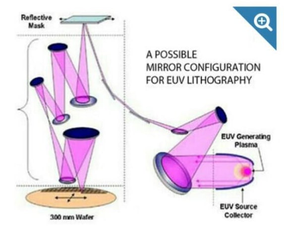
This superior DRAM is anticipated to unlock exponential development and alternatives for a rise within the digital financial system. It’s a main step to safe the semiconductor provide chain. At the moment, Micron is a pioneer in DRAM manufacturing. Lately, it put in excessive ultraviolet (EUV) lithography manufacturing gear at its A3 wafer fabrication unit in Taiwan.
In Could 2023, Micron introduced that it is going to be introducing this subtle sample know-how (EUV) to fabricate its next-generation DRAM, 1-gamma node. This know-how is anticipated to supply the smallest cell dimension for DRAM. The draw back of EUV lithography is that it wants multi-patterning, permitting 193nm lithography to significantly scale back the dimensions of DRAM. Micron is combining new supplies, instruments, and novel methods to enhance its multi-patterned alignment.
| Desk 1 SRAM Vs DRAM | ||
| Parameter | SRAM | DRAM |
| Learn/write velocity | Sooner | Slower than SRAM |
| Energy consumption | Extra | Much less |
| Inside construction | Advanced | Less complicated than SRAM |
| Density | Much less dense | Extremely dense |
| Utilized in | Cache reminiscence | Primary reminiscence |
| Storage per bit | Can retailer extra bits per chip | Can’t retailer many bits per chip |
| Storage part | Transistor | Capacitor |
| Value | Costly | Economical than SRAM |
Challenges Confronted by DRAM Trade
One-die Error Correction Code (ECC) is a particular function within the DRAM trade that corrects bit errors in DRAM chips, growing reliability and defect charges. ECC requires extra reminiscence storage the place ECC codes are saved on the time of reminiscence write to DRAM. Hamming codes are utilized in such ECC schemes to supply single-bit and double-bit error detection per burst. Newest DRAMs like LPDDR5 and DDR5 help one-die ECC.
Row hammer
The identical or adjoining rows are activated many times, leading to a loss or change of information contents within the rows that aren’t addressed. The most recent variations of DRAM LPDDR5/DDR5 help refresh administration (together with DRFM and ARFM) to compensate for this problem
System temperature
Customers have to verify with the DRAM vendor on the temperature vary the place DRAM ought to function. Knowledge integrity is misplaced at a stage higher than a sure temperature.
Lack of energy
DRAM might lose its contents because of a lack of energy. So, a backup non-volatile reminiscence is required the place DRAM contents should be copied earlier than the facility is misplaced. When energy is regained, saved contents in non-volatile reminiscence are written again to DRAM.
Specs of DDR5 and Lpddr5 as set by the Joint Electron System Engineering Council (JEDEC), which is an trade requirements physique and governs specs of DRAMs, are given in Desk 2.
| Desk 2 Specification of DDR5 and Lpddr5 | ||
| Issue | DDR5 | Lpddr5 |
| Most die density | 64Gbit | 32Gbit |
| Max. information charge | 6.4Gbps | 6.4Gbps |
| Max. UDIMM dimension (DSDR) | 128GB | N/A |
| Channels | 2 | 1 |
| Channel width | 64 bits (2×32) | 16 bits |
| Reminiscence banks | 4 | 16 |
| Financial institution teams | 08/04/23 | 4 |
| Burst size | BL 16×2 | BL 16 |
| Prefetch | 16n | 16n |
| Voltage( Vdd) | 1.1V | 1.05V |
| Vddq | 1V | 0.5V |
DDR5 MC and PHY
DDR5 is described because the fifth-generation Double Knowledge Price Synchronous DRAM designed for next-generation computing. DDR5 Reminiscence Controller (MC) and DDR PHY are two main elements for environment friendly DRAM efficiency. DDR5 MC wants digital design consultants whereas DDR5 PHY wants each digital and analogue experience. For every utility, DDR5 has a lot of timing parameters and configuration registers. Every vendor has to personal its personal distinctive timing parameter and configuration register values. DDR5 PHY Interface (DFI) is an interface protocol that defines timing, alerts, and programmable parameters required to switch information to and from DRAM to MC. In lots of conditions, MC and PHY are designed individually and infrequently by totally different firms.
Subsequent era DRAMs
Present DRAMs improve latency and energy consumption, generally known as the ‘reminiscence wall.’ Subsequent-generation DRAMs have give you new options to beat these challenges. Launched by Intel in 2015, 3D XPoint is described as the following era DRAM. 3D XPoint is predicated on a know-how referred to as Section-Change Reminiscence (PCM) and is utilized in SSDs and DIMMs. PCM shops data within the amorphous and crystalline phases.
In the meantime, the trade can be growing different new reminiscence sorts, reminiscent of Magnetoresistive RAM (MRAM) and Resistive RAM (ReRAM). Like 3D XPoint, MRAM and ReRAM could be made and offered as standalone gadgets.
3D XPoint shouldn’t be offered as an embedded reminiscence. In distinction, MRAM and ReRAM can even serve within the embedded reminiscence markets. For MRAM, the trade is growing a next-generation know-how referred to as Spin-Switch Torque MRAM (STT-MRAM). STT-MRAM makes use of the magnetism of electron spin to supply non-volatile properties in chips, combining the velocity of SRAM and the non-volatility of flash with limitless endurance.
In conventional reminiscence, information is saved as an electrical cost. In distinction, MRAM makes use of a magnetic tunnel junction (MTJ) reminiscence cell for the storage component. Ferroelectric RAM (FRAM) is one other know-how to observe. Utilizing a ferroelectric capacitor to retailer information, FRAM is a non-volatile reminiscence with massive storage capability. Nantero, a non-public firm, has greater than 170 nanotube patents to switch DRAMs. It’s doable to have tons of and 1000’s of such nanotubes in each reminiscence cell to kind a community of resistive parts to kind non-volatile random entry reminiscence (NVRAM). Undoubtedly, next-generation DRAMs are offering loads of alternatives for OEMs.
Our previous, current, and future reminiscence necessities within the e-world are way more than we anticipate. Within the net world, data could be saved alive by reminiscence. DRAM offers one other view of e-memory, offering one other understanding of the ‘information storage mechanism.’
The writer, Vinayak Ramachandra Adkoli, is BE in industrial manufacturing and has served as a lecturer in three totally different polytechnics for ten years. He’s additionally a contract author and cartoonist